|

| | The use of FPGAs has revolutionized the way DSP subsystems are configured. With a large number of gates, hardware multipliers and high-speed serial interfaces, an FPGA can outperform a microprocessor by a factor of ten or more. FPGAs are applicable to a variety of applications including RADAR, signal intelligence and image processing that have elements of computing that are characterized by repetitive fixed-point processing that can be expressed in highly parallel form. FFTs, pulse compression, filters, and digital down converters are examples of functions that FPGAs perform well. | 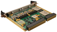
| In deployed systems, this technical advantage translates to smaller, lower-power and lower-cost systems. |
6U VPX/VXS-Based FPGA Product | Processor(s) | Memory | I/O | Ruggedization | CHAMP-FX3 (VPX6-472) | Freescale MPC8640D | 2 GB DDR3 SDRAM | N/A | AC 0, 100, CC 100, 200, 300 | CHAMP-FX2 VPX, Virtex5, 8641D | Dual-Core 8641D 1GHz, Dual Xilinx Virtex-5 LXT (LX110T, LX220T) | 8641: 512 MB or 1 GB DDR2 Across two banks, FPGAs: 512 MB DDR2 SDRAM across two banks per FPGA, 36 MB QDR-II+ SRAM per FPGA across four banks | Four 4-lane Serial RapidIO links, 8-lane PCIe or 4-lane SRIO XMC; Processor: 4-lane Serial RapidIO to Fabric, 1 x EIA-232, 1 x EIA-422/232, 2 x Gbe, 16 LTTL DIO; FPGAs: 4-lane Serial RapidIO to fabric, 4-lane RocketIO, 36-pairs LVDS DIO from each FPGA | AC 0, 100, CC 100, 200, 300 | FPE650 VPX Quad Virtex-5 | Quad Xilinx Virtex-5 (SX95T, LX155T or FX100T) FPGAs | FPGA 1&3: 2x 128Mx16-bit SDRAM, 2x 128Mx 24-bit SDRAM, 2x 4Mx18-bit SRAM, 128MB Flash; FPGA 2&4: 4x 4Mx18-bit SRAM | 2x FMCs, RocketIO, 20 Diff. Pairs for FPGAs 1 & 3, 4x Gbe | AC 0, CC 100 | HPE720 VPX, Virtex5, 8640 | 8640 or 8641 1GHz - 1.33GHz, 2x Virtex-5 FPGAs | 8641: 2GB DDR2 SDRAM, 128MB Flash and 128KB NvSRAM, per FPGA: 4x 9MB QDRII SRAM, 2x 512MB DDR2 and 16MB Flash | 2x FMC OR 1x FMC and 1 P/XMC, 2x Gbe onboard, RocketIO, 2x SRIO, 1x 8-lane PCIe | AC 0 | VPF2 VXS, Virtex5, 8641 | 8641D, 1x Virtex-5 FPGAs | 8641: 2GB DDR2 SDRAM and 128MB Flash, per FPGA: 4x 9MB QDRII SRAM, 2x 128MB DDR2 SDRAM, 32MB Flash | 1x P/XMC, 2x Gbe onboard, 1x EIA-232, RocketIO, VME | AC 0, CC 100 | VPF1 Dual PowerPC/FPGA | 2x 7447A/7448 1GHz, 2x Virtex-II Pro FPGAs | per 744x: 256MB SDRAM and 64MB Flash, per FPGA: 128MB DDR SDRAM and 4x 2MB QDR SRAM | 1 PMC, 2x EIA-422, 2x EIA-232, 2x Gbe onboard, RocketIO, VME | AC 0, CC 100 | CHAMP-FX Dual Virtex II Pro | Dual Xilinx VP70/100 | Up to 512 MB DDR SDRAM, Up to 9MB DDR-II SRAM per FPGA | 2 x 64-bit/66MHz PMC, 1 x EIA-232, StarFabric, RocketIO | AC 0, 100, CC 100, 200 |
3U VPX/VXS-Based FPGA Product | Processor(s) | Memory | I/O | Ruggedization | VPX3-450 VPX, Virtex5, 8640D | Dual-Core 8640D 1GHz, Xilinx Virtex-5 (LX155T or SX95T) | 8640: 1 GB DDR2 SDRAM Across two banks, FPGAs: 512 MB DDR2 SDRAM, 18 MB QDR-II+ SRAM across two banks | Two 4-lane PCI Express links (One link may be configured for Serial RapidIO) to backplane, 8-lane PCIe XMC, 2 x EIA-232, 2 x Gbe, 2 x 4-lane RocketIO to backplane, 18-pairs LVDS DIO | AC 0, 100, CC 100, 200 | FPE320 VPX Virtex-5 | Xilinx Virtex-5 (SX240T, 220/330T) FPGA | 2x 9MB QDR-II SRAM, 2x 356-512MB DDR2 SDRAM | 1x FMC, RocketIO, 16 Diff. Pairs, 1x EIA-232 | AC 0, 100,CC 200 | 3CPF1 PowerPC/FPGA | 7447A, Xilinx Virtex-II Pro XC2VP70 | 7447A: 512MB SDRAM, 64MB Flash; FPGA: 128MB SDRAM, 4x 4MB QDR SRAM | 1x EIA-232, 1x EIA-422, 1x I2O, RocketIO, 32-bit 33MHz PCI to backplane, 2x Ethernet | AC 0, CC 100 |
XMC-Based FPGA Product | Processor(s) | Memory | I/O | Ruggedization | ADX000 Virtex5 PMC/XMC | Xilinx Virtex-5 LX110T/SX95T FPGA | Dual banks of 36b QDR2 SRAM and 16b DDR2 SDRAM memories | N/A | AC L0, 100, CC 100 (contact factory for availability) | AD1520 1.5GSPS 8-bit ADC | Xilinx Virtex-5 LX110T/SX95T FPGA | Dual banks of QDR2 SRAM and DDR2 SDRAM memories | N/A | N/A | AD3000 3GSPS 8-bit ADC | Xilinx Virtex-5 LX110T/SX95T FPGA | Dual banks of QDR2 SRAM and DDR2 SDRAM memories | N/A | N/A | XMC-442 Virtex5 FPGA mezzanine | Single Xilinx Virtex-5 SXT (SX50T/SX95T) | Up to 256 MB DDR2 SDRAM, 18 MB SRAM Across two banks | 80-bits front-panel VDS/LVTTL (40 pairs), 48-bits rear-panel LVDS/LVTTL (24 pairs), x4 PCIe | AC 0, 100, CC 100, 200, 300 | XMC-FPGA05D Virtex-5 XMC/PMC | Xilinx Virtex-5 SX95T | Two banks of 9Mbytes 250MHz QDR2 SRAM memory; Two banks of 128Mbytes 250MHz DDR2 SDRAM memory | Range of front panel I/O personality modules (including ADC, DAC, LVDS, RS-485/422 and Camera Link) | N/A | XMC-FPGA05F Virtex-5 XMC | Xilinx® Virtex®-5 FPGA (SX95T, LX155T or FX100T) | Four banks of DDR SDRAM memory | 64-bit I/O arranged as 32 differential pairs connected directly to the FPGA | N/A |
PMC-Based FPGA Product | Processor(s) | Memory | I/O | Ruggedization | ADX000 Virtex5 PMC/XMC | Xilinx Virtex-5 LX110T/SX95T FPGA | Dual banks of 36b QDR2 SRAM and 16b DDR2 SDRAM memories | N/A | AC 0, 100, CC 100 (contact factory for availability) | PMC-FPGA03 Virtex-II Pro PMC | Xilinx Virtex-II Pro XC2VP50 | 2x 64MB DDR SDRAM, 3x 2Mx18-bit QDR-II SRAM | 138 Signals to front panel or RocketIO to front panel, 64-bit 66MHz PCI, 64-bit User I/O on PMC P14 | AC 0 | PMC-FPGA03F Quad Virtex-II Pro PMC | Xilinx Virtex-II Pro XC2VP50 | 2x 64MB DDR SDRAM, 3x 2Mx18-bit QDR-II SRAM | 4 fiber-optic on front panel, 64-bit 66MHz PCI, 64-bit User I/O on PMC P14 | AC 0 | PMC-FPGA05 Virtex5 PMC | Xilinx Virtex-5 LX110 or LX155 FPGA | Multiple banks of SRAM for DSP; Multiple banks of SDRAM for large buffers | Customizable digital I/O | N/A | PMC-FPGA05D Virtex-5 XMC/PMC | Xilinx Virtex-5 SX95T | Two banks of 9Mbytes 250MHz QDR2 SRAM memory; Two banks of 128Mbytes 250MHz DDR2 SDRAM memory | Range of front panel I/O personality modules (including ADC, DAC, LVDS, RS-485/422 and Camera Link) | N/A | PMC-440 Virtex-II Pro | Xilinx VP40 | Up to 256 MB DDR SDRAM | 33/66 MHz PCI, 2.5 GB/sec Front-panel RocketIO, 2 GB/sec Rear-panel RocketIO, 30-bits front-panel LVDS/LVTTL (15 pairs), 48-bits rear-panel LVDS/LVTTL (24 pairs) | AC 0, 100, CC 100, 200 |
|